- 您现在的位置:买卖IC网 > Sheet目录2005 > LTC2143CUP-14#PBF (Linear Technology)IC ADC DUAL 14BIT 80 MSPS 64-QFN
29
21454314fa
LTC2145-14/
LTC2144-14/LTC2143-14
APPLICATIONS INFORMATION
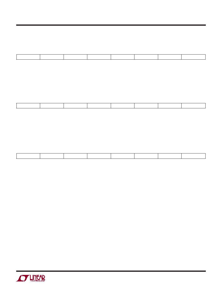
Table 3. Serial Programming Mode Register Map (PAR/SER = GND)
REGISTER A0: RESET REGISTER (ADDRESS 00h)
D7
D6
D5
D4
D3
D2
D1
D0
RESET
XXXXXX
X
Bit 7
RESET
Software Reset Bit
0 = Not Used
1 = Software Reset. All Mode Control Registers Are Reset to 00h. The ADC is momentarily placed in SLEEP mode. This bit is
automatically set back to zero at the end of the SPI write command. The reset register is write only. Data read back from the reset
register will be random.
Bits 6-0
Unused, Don’t Care Bits.
REGISTER A1: POWER-DOWN REGISTER (ADDRESS 01h)
D7
D6
D5
D4
D3
D2
D1
D0
XXXXXX
PWROFF1
PWROFF0
Bits 7-2
Unused, Don’t Care Bits.
Bits 1-0
PWROFF1:PWROFF0
Power Down Control Bits
00 = Normal Operation
01 = Channel 1 in Normal Operation, Channel 2 in Nap Mode
10 = Channel 1 and Channel 2 in Nap Mode
11 = Sleep Mode
REGISTER A2: TIMING REGISTER (ADDRESS 02h)
D7
D6
D5
D4
D3
D2
D1
D0
XXXX
CLKINV
CLKPHASE1
CLKPHASE0
DCS
Bits 7-4
Unused, Don’t Care Bits.
Bit 3
CLKINV
Output Clock Invert Bit
0 = Normal CLKOUT Polarity (As Shown in the Timing Diagrams)
1 = Inverted CLKOUT Polarity
Bits 2-1
CLKPHASE1:CLKPHASE0
Output Clock Phase Delay Bits
00 = No CLKOUT Delay (As Shown in the Timing Diagrams)
01 = CLKOUT+/CLKOUT– Delayed by 45° (Clock Period 1/8)
10 = CLKOUT+/CLKOUT– Delayed by 90° (Clock Period 1/4)
11 = CLKOUT+/CLKOUT– Delayed by 135° (Clock Period 3/8)
Note: If the CLKOUT Phase Delay Feature Is Used, the Clock Duty Cycle Stabilizer Must Also Be Turned On
Bit 0
DCS
Clock Duty Cycle Stabilizer Bit
0 = Clock Duty Cycle Stabilizer Off
1 = Clock Duty Cycle Stabilizer On
发布紧急采购,3分钟左右您将得到回复。
相关PDF资料
LTC2153IUJ-14#PBF
IC ADC 14BIT DUAL 310MSPS 40QFN
LTC2158IUP-14#TRPBF
IC ADC DUAL 14BIT 310M 64-QFN
LTC2172IUKG-14#TRPBF
IC ADC 14BIT SER/PAR 65M 52-QFN
LTC2175IUKG-14#TRPBF
IC ADC 14BIT 125MSPS QUAD 52QFN
LTC2202IUK#TRPBF
IC ADC 16-BIT 10MSPS 48-QFN
LTC2205IUK-14#PBF
IC ADC 14BIT 65MSPS 48-QFN
LTC2207IUK-14#PBF
IC ADC 14BIT 105MSPS 48-QFN
LTC2220IUP-1#TRPBF
IC ADC 12BIT 185MSPS 64-QFN
相关代理商/技术参数
LTC2143CUP-14#TRPBF
功能描述:IC ADC DUAL 14BIT 80 MSPS 64-QFN RoHS:是 类别:集成电路 (IC) >> 数据采集 - 模数转换器 系列:- 标准包装:1 系列:- 位数:14 采样率(每秒):83k 数据接口:串行,并联 转换器数目:1 功率耗散(最大):95mW 电压电源:双 ± 工作温度:0°C ~ 70°C 安装类型:通孔 封装/外壳:28-DIP(0.600",15.24mm) 供应商设备封装:28-PDIP 包装:管件 输入数目和类型:1 个单端,双极
LTC2143IUP-12#PBF
功能描述:IC ADC DUAL 12BIT 80MSPS 64-QFN RoHS:是 类别:集成电路 (IC) >> 数据采集 - 模数转换器 系列:- 标准包装:1 系列:- 位数:14 采样率(每秒):83k 数据接口:串行,并联 转换器数目:1 功率耗散(最大):95mW 电压电源:双 ± 工作温度:0°C ~ 70°C 安装类型:通孔 封装/外壳:28-DIP(0.600",15.24mm) 供应商设备封装:28-PDIP 包装:管件 输入数目和类型:1 个单端,双极
LTC2143IUP-12#TRPBF
功能描述:IC ADC DUAL 12BIT 80MSPS 64-QFN RoHS:是 类别:集成电路 (IC) >> 数据采集 - 模数转换器 系列:- 标准包装:1 系列:- 位数:14 采样率(每秒):83k 数据接口:串行,并联 转换器数目:1 功率耗散(最大):95mW 电压电源:双 ± 工作温度:0°C ~ 70°C 安装类型:通孔 封装/外壳:28-DIP(0.600",15.24mm) 供应商设备封装:28-PDIP 包装:管件 输入数目和类型:1 个单端,双极
LTC2143IUP-14#PBF
功能描述:IC ADC DUAL 14BIT 80 MSPS 64-QFN RoHS:是 类别:集成电路 (IC) >> 数据采集 - 模数转换器 系列:- 标准包装:1 系列:- 位数:14 采样率(每秒):83k 数据接口:串行,并联 转换器数目:1 功率耗散(最大):95mW 电压电源:双 ± 工作温度:0°C ~ 70°C 安装类型:通孔 封装/外壳:28-DIP(0.600",15.24mm) 供应商设备封装:28-PDIP 包装:管件 输入数目和类型:1 个单端,双极
LTC2143IUP-14#TRPBF
功能描述:IC ADC DUAL 14BIT 80 MSPS 64-QFN RoHS:是 类别:集成电路 (IC) >> 数据采集 - 模数转换器 系列:- 标准包装:1 系列:- 位数:14 采样率(每秒):83k 数据接口:串行,并联 转换器数目:1 功率耗散(最大):95mW 电压电源:双 ± 工作温度:0°C ~ 70°C 安装类型:通孔 封装/外壳:28-DIP(0.600",15.24mm) 供应商设备封装:28-PDIP 包装:管件 输入数目和类型:1 个单端,双极
LTC2144-12
制造商:LINER 制造商全称:Linear Technology 功能描述:12-Bit, 125Msps/105Msps/ 80Msps Low Power Dual ADCs
LTC2144-14
制造商:LINER 制造商全称:Linear Technology 功能描述:12-Bit, 125Msps/105Msps/ 80Msps Low Power Dual ADCs
LTC2144CUP-12#PBF
功能描述:IC ADC DUAL 12BIT 105MSPS 64-QFN RoHS:是 类别:集成电路 (IC) >> 数据采集 - 模数转换器 系列:- 标准包装:1 系列:- 位数:14 采样率(每秒):83k 数据接口:串行,并联 转换器数目:1 功率耗散(最大):95mW 电压电源:双 ± 工作温度:0°C ~ 70°C 安装类型:通孔 封装/外壳:28-DIP(0.600",15.24mm) 供应商设备封装:28-PDIP 包装:管件 输入数目和类型:1 个单端,双极